


 购物车0
购物车0元器件商品{{ gnNumber + hkNumber }}
国内交货{{ gnNumber }}香港交货{{ hkNumber }}
购物车中还没有商品,赶紧选购吧


dsPIC33F General Purpose Digital Signal Controller (DSC) with seamless migration options to PIC24F, PIC24H MCUs and dsPIC30F DSCs in similar packages
Operating Range:DC – 40 MIPS (40 MIPS @ 3.0-3.6V, -40°C to +125°C)
Industrial temperature range (-40°C to +85°C)
Extended temperature range (-40°C to +125°C)
High-Performance DSC CPU:Modified Harvard architecture
C compiler optimized instruction set
16-bit wide data path
24-bit wide instructions
Linear program memory addressing up to 4M instruction words
Linear data memory addressing up to 64 Kbytes
83 base instructions: mostly 1 word/1 cycle
Sixteen 16-bit General Purpose Registers
Two 40-bit accumulators:
With rounding and saturation options
Flexible and powerful addressing modes:
Indirect, Modulo and Bit-Reversed
Software stack
16 x 16 fractional/integer multiply operations
32/16 and 16/16 divide operations
Single-cycle multiply and accumulate:
Accumulator write back for DSP operations
Dual data fetch
Up to ±16-bit shifts for up to 40-bit data
Direct Memory Access (DMA):8-channel hardware DMA
2 Kbytes dual ported DMA buffer area (DMA RAM) to store data transferred via DMA:
Allows data transfer between RAM and a peripheral while CPU is executing code (nocycle stealing)
Most peripherals support DMA Interrupt Controller
5-cycle latency
118 interrupt vectors
Up to 67 available interrupt sources
Up to 5 external interrupts
7 programmable priority levels
5 processor exceptions
Digital I/O:Wake-up/Interrupt-on-Change on up to 24 pins
Output pins can drive from 3.0V to 3.6V
All digital input pins are 5V tolerant
4 mA sink on all I/O pins
System Management:Flexible clock options:
External, crystal, resonator, internal RC
Fully integrated PLL
Extremely low jitter PLL
Power-up Timer
Oscillator Start-up Timer/Stabilizer
Watchdog Timer with its own RC oscillator
Fail-Safe Clock Monitor
Reset by multiple sources Power Management
On-chip 2.5V voltage regulator
Switch between clock sources in real time
Idle, Sleep and Doze modes with fast wake-up
Timers/Capture/Compare/PWM:Timer/Counters, up to nine 16-bit timers:
Can pair up to make four 32-bit timers
1 timer runs as Real-Time Clock with external 32.768 kHz oscillator
Programmable prescaler
Input Capture (up to 8 channels):
Capture on up, down or both edges
16-bit capture input functions
4-deep FIFO on each capture
Output Compare (up to 8 channels):
Single or Dual 16-Bit Compare mode
16-bit Glitchless PWM mode
Communication Modules:3-wire SPI (up to 2 modules):
Framing supports I/O interface to simple codecs
Supports 8-bit and 16-bit data
Supports all serial clock formats and sampling modes
I2C™ (up to 2 modules):
Full Multi-Master Slave mode support
7-bit and 10-bit addressing
Bus collision detection and arbitration
Integrated signal conditioning
Slave address masking
UART (up to 2 modules):
Interrupt on address bit detect
Interrupt on UART error
Wake-up on Start bit from Sleep mode
4-character TX and RX FIFO buffers
LIN bus support
IrDA® encoding and decoding in hardware
High-Speed Baud mode
Hardware Flow Control with CTS and RTS
Data Converter Interface (DCI) module:
Codec interface
Supports I2S and AC’97 protocols
Up to 16-bit data words, up to 16 words per frame
4-word deep TX and RX buffers
Enhanced CAN (ECAN™ module) 2.0B active (up to 2 modules):
Up to 8 transmit and up to 32 receive buffers
16 receive filters and 3 masks
Loopback, Listen Only and Listen All Messages modes for diagnostics and bus monitoring
Wake-up on CAN message
Automatic processing of Remote Transmission Requests
FIFO mode using DMA
DeviceNet™ addressing support
Analog-to-Digital Converters (ADCs):Up to two ADC modules in a device
10-bit, 1.1 Msps or 12-bit, 500 Ksps conversion:
2, 4 or 8 simultaneous samples
Up to 32 input channels with auto-scanning
Conversion start can be manual or synchronized with 1 of 4 trigger sources
Conversion possible in Sleep mode
±2 LSb max integral nonlinearity
±1 LSb max differential nonlinearity CMOS Flash Technology
Low-power, high-speed Flash technology
Fully static design
3.3V (±10%) operating voltage
Industrial temperature
Low-power consumption
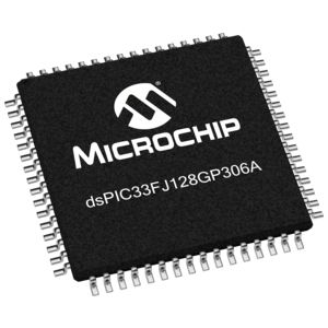
DSPIC33FJ128GP306A 封装图
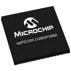
DSPIC33FJ128GP306A 封装图
DSPIC33FJ128GP306A 封装图
DSPIC33FJ128GP306A 封装图
DSPIC33FJ128GP306A 封装图
DSPIC33FJ128GP306A 封装图
| 型号 | 制造商 | 描述 | 购买 |
|---|---|---|---|
| DSPIC33FJ128GP306AT-E/PT | AVX | 220 pF ±20% 2000V(2kV) 陶瓷电容器 X7R 1206(3216 公制) | 立即购买 |
| DSPIC33FJ128GP306AT-E/MR | AVX | 100 pF ±10% 3000V(3kV) 陶瓷电容器 C0G,NP0 1812(4532 公制) | 立即购买 |
| DSPIC33FJ128GP306AT-I/PT | Sanyo Denki | 40MMSTANDARDFANGUARDS | 立即购买 |
| DSPIC33FJ128GP306AT-I/MR | Laird Technologies Thermal Materials | TGREASE300X3KGCAN1GAL | 立即购买 |
| DSPIC33FJ128GP306A-E/PT | ATS | HEATSINK45X45X20MMR-TABCP | 立即购买 |
| DSPIC33FJ128GP306A-E/MR | Wakefield-Vette | HEATSINKPINFIN21X21MMCLIP | 立即购买 |
深入探讨Microchip的dsPIC33FJ16(GP/MC)101/102和dsPIC33FJ32(GP/MC)101/102/104这两款16位数字信号控制器,看看它们有哪些独特的特性和应用场
公司推出的 dsPIC33EPXXXGM3XX/6XX/7XX 16 位数字信号控制器,看看它有哪些强大的功能和特性。 文件下载: DSPIC33EP128GM306-I/PT.pdf 一、器件概述
dsPIC33FJ系列16位数字信号控制器深度解析 在电子工程师的设计工作中,选择合适的控制器是项目成功的关键。今天我们来深入探讨Microchip的dsPIC33FJ16(GP/MC)101
...备的保护电源。本文介绍了UPS参考设计的主要指标,采用dsPIC33FJ16GS504的离线UPS机箱图,电路图,材料清单和PCB元件布局图。
dsPIC33FJ06GS101/X02和dsPIC33FJ16GSX02/X04数字信号控制器:设计指南与特性解析 一、引言 在电子设计领域,数字信号控制器(DSC)的性能和功能对于众多
的 dsPIC33FJ32GP302/304、dsPIC33FJ64GPX02/X04 和 dsPIC33FJ128GPX02/X04 这几款 16 位数字信号控制器。 文件下载: DSPIC33FJ128GP
探索Microchip dsPIC33FJ12GP201/202:高性能16位数字信号控制器 在电子工程师的工具箱中,高性能的数字信号控制器(DSC)是实现复杂控制和信号处理任务的关键组件
的 dsPIC33FJ32GP302/304、dsPIC33FJ64GPX02/X04 和 dsPIC33FJ128GPX02/X04 这三款 16 位数字信号控制器。它们集成了先进的模拟功能,适用于多种应用场
 上传BOM
上传BOM

 工商网监
工商网监