


 购物车0
购物车0元器件商品{{ gnNumber + hkNumber }}
国内交货{{ gnNumber }}香港交货{{ hkNumber }}
购物车中还没有商品,赶紧选购吧


制造商:ON
MC14049B电路图
| 型号 | 制造商 | 描述 | 购买 |
|---|---|---|---|
| NLV14049BDR2G | ON | NLV14049BDR2G | 立即购买 |
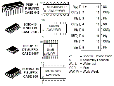
| MC14049BDG | ON | MC14049B 六反相器/缓冲器和 MC14050B 六同相缓冲器采用 MOS P 沟道和 N 沟道增强型器件,集成于单一单片结构中。这些互补 MOS 器件主要用于需要低功耗和/或高抗噪性的场合。这些器件仅使用一个电源电压 VDD 即可实现逻辑电平转换 | 立即购买 |
| MC14049BDR2G | ON | MC14049B 六反相器/缓冲器和 MC14050B 六同相缓冲器采用 MOS P 沟道和 N 沟道增强型器件,集成于单一单片结构中。这些互补 MOS 器件主要用于需要低功耗和/或高抗噪性的场合。这些器件仅使用一个电源电压 VDD 即可实现逻辑电平转换 | 立即购买 |
| 标题 | 类型 | 大小(KB) | 下载 |
|---|---|---|---|
| Hex Buffer | 125 | 点击下载 | |
| SOIC 16 LEAD | 37 | 点击下载 | |
| MC14049B_PKG.GIF | UNKNOW | 16 | 点击下载 |
MC3303DG是什么芯片? ; MC3303DG是一种多路运算放大器(op amp)芯片。多路运算放大器是一种电子元件,通常用于信号放大、滤波和运算。MC3303DG是一款集成了四个独立的操作
MC3363接收电路
MC34063是单片双极型线性集成电路,片内包含有温度补偿带隙基准源、一个占空比周期控制振荡器、驱动器和大电流输出开关管,能输出1.5A的开关电源。
3只锂电池串联后的电压约12V,要为其充电,要用12.6V的充电器,而这种充电器不易买到。
探索MC14008B 4位全加器:特性、参数与应用 在电子设计的世界里,加法器是构建数字电路的基础组件之一。今天,我们就来深入了解一款经典的4位全加器——MC14008B。 文件下载
深入解析MC14538B:双精度可重触发/可复位单稳态多谐振荡器 在电子工程师的日常设计工作中,单稳态多谐振荡器是一种常用的电路元件,它能够产生精确的脉冲信号,广泛应用于各种定时、计数和控制电路中
4.70 GHz 表面贴装带通滤波器 B047MC5S:5G 频段的理想之选 在 5G 技术飞速发展的今天,对于高性能滤波器的需求日益增长。今天要为大家介绍的是 DLI 推出的 4.70 GHz
MC13135内含振荡器、VCO变容调谐二极管、低噪声第一和第二混频器及LO、高性能限幅放大器、RSSI。其中提供LC积分检波器,为RSSI缓冲器和数据比较器设置了一级运算放大级。
 上传BOM
上传BOM

 工商网监
工商网监