
 购物车0
购物车0元器件商品{{ gnNumber + hkNumber }}
国内交货{{ gnNumber }}香港交货{{ hkNumber }}
购物车中还没有商品,赶紧选购吧


制造商:TI
The LF298 and LFx98x devices are monolithic sample-and-hold circuits that use BI-FET technology to obtain ultrahigh DC accuracy with fast acquisition of signal and low droop rate. Operating as a unity-gain follower, DC gain accuracy is 0.002% typical and acquisition time is as low as 6 µs to 0.01%. A bipolar input stage is used to achieve low offset voltage and wide bandwidth. Input offset adjust is accomplished with a single pin and does not degrade input offset drift. The wide bandwidth allows the LF198-N to be included inside the feedback loop of 1-MHz operational amplifiers without having stability problems. Input impedance of 1010 Ω allows high-source impedances to be used without degrading accuracy.
P-channel junction FETs are combined with bipolar devices in the output amplifier to give droop rates as low as 5 mV/min with a 1-µF hold capacitor. The JFETs have much lower noise than MOS devices used in previous designs and do not exhibit high temperature instabilities. The overall design ensures no feedthrough from input to output in the hold mode, even for input signals equal to the supply voltages.
Logic inputs on the LF198-N are fully differential with low input current, allowing for direct connection to TTL, PMOS, and CMOS. Differential threshold is
1.4 V. The LF198-N will operate from ±5-V to ±18-V supplies.
An A version is available with tightened electrical specifications.
Operates from ±5-V to ±18-V Supplies
Less than 10-µs Acquisition Time
Logic Input Compatible With TTL, PMOS, CMOS
0.5-mV Typical Hold Step at Ch = 0.01 µF
Low Input Offset
0.002% Gain Accuracy
Low Output Noise in Hold Mode
Input Characteristics Do Not Change During Hold Mode
High Supply Rejection Ratio in Sample or Hold
Wide Bandwidth
Space Qualified, JM38510


LF398-N 封装图
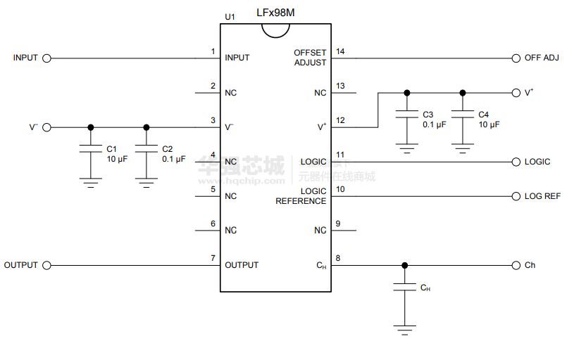
LF398-N 封装图
LF398-N电路图

LF398-N 引脚图
| 型号 | 制造商 | 描述 | 购买 |
|---|---|---|---|
| LF398N/NOPB | TI | LF398-N 单片采样保持电路(10μs 采集,7mV 失调电压) | 立即购买 |
| LF398M | TI | 立即购买 | |
| LF398AN/NOPB | TI | 采样和保持 放大器 1 电路 8DIP | 立即购买 |
| LF398M/NOPB | TI | LF398-N 单片采样保持电路(10μs 采集,7mV 失调电压) | 立即购买 |
| LF398MX/NOPB | TI | LF398-N 单片采样保持电路(10μs 采集,7mV 失调电压) | 立即购买 |
| - | - | 立即购买 |
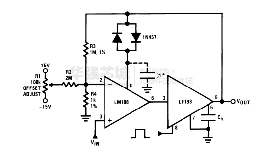
峰值电压采样保持电路:峰值电压采样保持电路如图12-50所示。峰值电压采样保持电路南一片采样保持器芯片LF398和一块电压比较器LM311构成。LF398的输出电压和输入电压通过LM3J1进行比较t当U.》Uo时.
由于成本上的优势,目前市场上的NAND闪存主流已经变成了TLC、QLC,MLC都很罕见了,SLC闪存更是凤毛麟角,消费级市场上几乎消失了。
意法半导体 STL320N4LF8 N沟道STripFET F8功率MOSFET 采用STripFET F8沟槽式MOSFET技术制造而成。 该器件完全符合工业级标准。STL320N4LF8可降低
意法半导体STL325N4LF8AG N沟道功率MOSFET采用STripFET F8技术,具有增强型沟槽栅极结构。 STL325N4LF8AG可确保非常低的导通电阻。该器件还降低内部电容和栅极电荷,实现更快、更高效的开关。
摘要 :本文介绍了一种以采样/ 保持器 L F398 芯片为主要器件的峰值保持电路。该电路具有结构简单、调试方便、性能优良等优点 ,可广泛应用于各种脉冲分析系统。
两个采样保持放大器LF398构成的阶梯波发生电路图 如图所示为由两个LF398构成的阶梯波发生电路。初始状态:两个
lf198/lf298/lf398应用电路
在A/D转换后能跟踪输入信号的变化。能完成这种功能的器件叫采样/保持器。采样/保持器在保持阶段相当于一个“模拟信号存储器”。
| LC823425 | LM1086-MIL | LM2595 | LM311 |
| LV8736V | LC87F2J32A | LIS2DS12 | LC75843UGA |
| LM4040 | LA5774MC | LM2991QML | LV52204MU |
| LB1876 | LB1843V | LC75056PE | LTST-C191KFKT |
| LMC6001-MIL | LM317M | LV8806QA | LM5175 |
 上传BOM
上传BOM

 工商网监
工商网监