
 购物车0
购物车0元器件商品{{ gnNumber + hkNumber }}
国内交货{{ gnNumber }}香港交货{{ hkNumber }}
购物车中还没有商品,赶紧选购吧


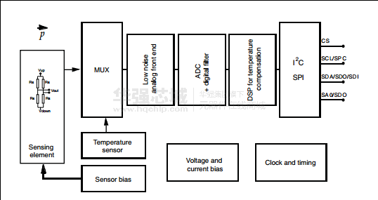
The LPS331AP is an ultra compact absolute piezoresistive pressure sensor. It includes a monolithic sensing element and an IC interface able to take the information from the sensing element and to provide a digital signal to the external world.
The sensing element consists of a suspended membrane realized inside a single mono-silicon substrate. It is capable to detecting pressure and is manufactured using a dedicated process developed by ST, called VENSENS.
The VENSENS process allows to build a mono-silicon membrane above an air cavity with controlled gap and defined pressure. The membrane is very small compared to the traditionally built silicon micromachined membranes. Membrane breakage is prevented by an intrinsic mechanical stopper.
The IC interface is manufactured using a standard CMOS process that allows a high level of integration to design a dedicated circuit which is trimmed to better match the sensing element characteristics.
The LPS331AP is available in a small holed cap land grid array (HCLGA) package and it is guaranteed to operate over a temperature range extending from -40 °C to +85 °C. The package is holed to allow external pressure to reach the sensing element.
lps331ap是一种超小型绝对压阻式压力传感器。它包括一个单片传感元件和一个集成电路接口能够从传感元件的信息,并提供一个数字信号到外部世界。
该传感元件由一个单一的单体硅衬底上实现的悬浮膜。它能够检测压力,使用专用的过程由ST开发制造,称为vensens。
的vensens过程允许建立一个单一的硅膜上方空气腔间隙和压力控制的定义。与传统的硅微机械膜相比,该膜是非常小的。防止膜破裂的内在机械塞。
IC接口采用标准的CMOS工艺,允许高层次的集成设计专用电路,修整,以更好地匹配传感元件特性制造。
在一个小的lps331ap孔帽栅格阵列是可用的(hclga)封装,这是保证工作在扩展温度范围从- 40°C + 85°C.包装孔允许外部压力达到传感元件。
260 to 1260 mbar absolute pressure range
High-resolution mode: 0.020 mbar RMS
Low power consumption:
Low resolution mode: 5.5 μA
High resolution mode: 30 μA
High overpressure capability: 20x full scale
Embedded temperature compensation
Embedded 24-bit ADC
Selectable ODR from 1 Hz to 25 Hz
SPI and I2C interfaces
Supply voltage: 1.71 to 3.6 V
High shock survivability: 10,000 g
Small and thin package
ECOPACK® lead-free compliant
主要特点
260到1260毫巴绝对压力范围
高分辨率模式:0.020 mbar RMS
低功耗:
低分辨模式:5.5
高分辨模式:30
高过压能力:20X全面
嵌入式温度补偿
嵌入式24位ADC
可选的ODR从1赫兹到25赫兹
SPI和I2C接口
电源电压:1.71至3.6伏
高冲击生存能力:10000克
小而薄的包装
®ECOPACK无铅兼容
LPS331AP电路图

LPS331AP 引脚图

LPS331AP 封装图

LPS331AP 封装图
...车辆中,人类与汽车之间的人机界面至关重要!近日, ALPS (阿尔卑斯电气)亮相 2018 年慕尼黑上海电子展 (electronica China 2018) ,分享了 ALPS 在人机界面、传感器和连接等方面的技术。
麦姆斯咨询:通过Alps与Greina签订的股份收购协议,Alps旨在通过整合基于Greina算法的高精度定位技术和Alps紧凑的高性能无线通讯模组技术,为汽车市场以及消费类电子产品和智能手机市场的传感解决方案提供更高的附加值。
CEATEC(日本电子高新科技博览会)是亚洲和日本国内电子领域最前沿、规模最大、产品范围最广的世界级展览会。10月4日~7日,CEATEC JAPAN 2016在幕张MESSE国际会展中心如期举行。据悉,2016年的参观人数与2015年相比,增加了9.1%。另外...
最近,ST意法半导体推出最新一代低功耗蓝牙系统芯片BlueNRG-LPS,这是一款超低功耗的可编程BluetoothLowEnergy无线SoC解决方案。BlueNRG-LPS符合
日前,ALPS公司开发出适用于车内空调、音响设备操作部的中空轴编码器。现今,通过采用旋钮式调控装置操作车内设备的需求仍不断扩大,为满足主副驾座各自独立调控,中央部分操作开关与液晶屏设计要求,需要扩大编码器...
ALPS Electric是日本一家以生产销售开关、传感器等为主的电气株式会社。近日,Alps开发了一种可以应用于VR领域的触觉反馈设备,该设备不仅适用于VR游戏,还能对医疗、维修等领域起到一定帮助。
意法半导体(ST)日前最新推出的微机电系统(MEMS)LPS001WP,该压力感测器成功实现智慧型手机以及其它可携式装置能够确
什么是LPSDRAM ,低功耗同步动态随机存取存储器。 LPRAM 相关介绍: LPSRAM又称为极快的低功耗SRAM,它可减少移
| LC75847T | LB11620T | LV8161MU | LA6597FMC |
| LV5725JA | LB11660RV | LM235 | LND150 |
| LM1458-MIL | LIS3DH | LM2902V | LM431SB |
| LMK04828 | LA5756 | LB11850VA | LMG3410 |
| LA5724MC | LF156QML | LM311-N | LB1843V |
 上传BOM
上传BOM

 工商网监
工商网监