
 购物车0
购物车0元器件商品{{ gnNumber + hkNumber }}
国内交货{{ gnNumber }}香港交货{{ hkNumber }}
购物车中还没有商品,赶紧选购吧


制造商:ADI/AD
优势和特点
JESD204B (Subclass 1) coded serial digital outputs
Lane rates up to 16 Gbps
1.6 W total power at 1300 MSPS
800 mW per ADC channel
SNR = 65.6 dBFS at 172 MHz (1.59 V p-p input range)
SFDR = 78 dBFS at 172.3 MHz (1.59 V p-p input range)
Noise density
−153.9 dBFS/Hz (1.59 V p-p input range)
−155.6 dBFS/Hz (2.04 V p-p input range)
0.95 V, 1.8 V, and 2.5 V supply operation
No missing codes
Internal ADC voltage reference
Flexible input range
1.36 V p-p to 2.04 V p-p (1.59 V p-p typical)
2 GHz usable analog input full power bandwidth
>95 dB channel isolation/crosstalk
Amplitude detect bits for efficient AGC implementation
2 integrated digital downconverters per ADC channel
48-bit NCO
Programmable decimation rates
Differential clock input
SPI control
Integer clock divide by 2 and divide by 4
Flexible JESD204B lane configurations
On-chip dithering to improve small signal linerarity
产品详情
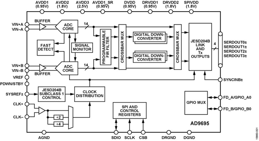
The AD9695 is a dual, 14-bit, 1300 MSPS/625 MSPS analog-todigitalconverter (ADC). The device has an on-chip buffer and asample-and-hold circuit designed for low power, small size, andease of use. This product is designed to support communicationsapplications capable of direct sampling wide bandwidth analogsignals of up to 2 GHz. The −3 dB bandwidth of the ADC inputis 2 GHz. The AD9695 is optimized for wide input bandwidth,high sampling rate, excellent linearity, and low power in a smallpackage.
The dual ADC cores feature a multistage, differential pipelinedarchitecture with integrated output error correction logic. EachADC features wide bandwidth inputs supporting a variety ofuser-selectable input ranges. An integrated voltage referenceeases design considerations. The analog input and clock signalsare differential inputs. The ADC data outputs are internallyconnected to four digital downconverters (DDCs) through acrossbar mux. Each DDC consists of multiple signal processingstages: a 48-bit frequency translator (numerically controlledoscillator (NCO)), and decimation filters. The NCO has the optionto select up to 16 preset bands over the general-purpose input/output (GPIO) pins, or use a coherent fast frequency hoppingmechanism for band selection. Operation of the AD9695 betweenthe DDC modes is selectable via SPI-programmable profiles.
In addition to the DDC blocks, the AD9695 has several functionsthat simplify the automatic gain control (AGC) function in acommunications receiver. The programmable threshold detectorallows monitoring of the incoming signal power using the fastdetect control bits in Register 0x0245 of the ADC. If the inputsignal level exceeds the programmable threshold, the fast detectindicator goes high. Because this threshold indicator has lowlatency, the user can quickly turn down the system gain to avoidan overrange condition at the ADC input. In addition to the fastdetect outputs, the AD9695 also offers signal monitoringcapability. The signal monitoring block provides additionalinformation about the signal being digitized by the ADC.
The user can configure the Subclasss 1 JESD204B-based highspeed serialized output using either one lane, two lanes, or fourlanes, depending on the DDC configuration and the acceptablelane rate of the receiving logic device. Multidevice synchronizationis supported through the SYSREF± and SYNCINB± input pins.The AD9695 has flexible power-down options that allowsignificant power savings when desired. All of these features canbe programmed using a 3-wire serial port interface (SPI) and orPDWN/STBY pin.
The AD9695 is available in a Pb-free, 64-lead LFCSP and isspecified over the −40°C to +105°C junction temperature range.This product may be protected by one or more U.S. orinternational patents.
Note that, throughout this data sheet, multifunction pins, suchas FD_A/GPIO_A0, are referred to either by the entire pinname or by a single function of the pin, for example, FD_A,when only that function is relevant.
Product Highlights
Low power consumption per channel.
JESD204B lane rate support up to 16 Gbps.
Wide, full power bandwidth supports intermediate
frequency (IF) sampling of signals up to 2 GHz.Buffered inputs ease filter design and implementation.
Four integrated wideband decimation filters and NCO
blocks supporting multiband receivers.Programmable fast overrange detection.
On-chip temperature diode for system thermal management.
Applications
Communications
Diversity multiband, multimode digital receivers
3G/4G, TD-SCDMA, WCDMA, GSM, LTE
General-purpose software radios
Ultrawideband satellite receiver
Instrumentation
Oscilloscopes
Spectrum analyzers
Network analyzers
Integrated RF test solutions
Radar
Electronic support measures, electronic counter measures, and electronic counter-counter measures
High speed data acquisition systems
DOCSIS 3.0 CMTS upstream receive paths
Hybrid fiber coaxial digital reverse path receivers
Wideband digital predistortion

AD9695 引脚图
AD9695电路图
| 型号 | 制造商 | 描述 | 购买 |
|---|---|---|---|
| AD9695BCPZRL7-625 | - | - | 立即购买 |
| AD9695BCPZRL7-1300 | - | - | 立即购买 |
| AD9695BCPZ-625 | - | - | 立即购买 |
| AD9695BCPZ-1300 | - | - | 立即购买 |
意法半导体(ST)作为世界领先的半导体供应商,凭借多年的经验和先进的技术创新为客户提供解决方案。丰富的产品类别,涵盖汽车、工业、通信设备、计算机及外设以及个人电子终端市场。
超级电容器由于其独特的物理和化学特性,可以被串联使用以适应不同的电源需求。
# 【技术分享】远程透传网关-单网口快速实现汇川PLC-AutoShop程序远程上下载
在电动汽车(EV)动力总成中讨论更激烈的部件旁边是机电开关,称为接触器。尽管它们在引擎盖下平淡无奇,但它们是保持电动汽车平稳运行的功能和安全要素的一部分。鉴于 41 年电动汽车注册量增长了 2020%1,并且每辆车都有几个接触器,这确实是一个重要的组件部分。
丁晖总结,生物医药产业已经成为海南自贸港主要战略产业,也是海口经济的重要支撑。近些年,海口生物医药产业迅猛崛起,年均增长率达到两位数,是工业领域中最为迅速、稳健的行业。
为满足光伏追踪系统对高压电源自带供电+充电功能的需求,金升阳使用自主技术,推出200-1200VDC超宽超高输入、输出端自带恒流充电功能的高压电源PV180-27A2828-BAT。
厚度可达3-50u”,因其优越的导电性、抗氧化性以及耐磨性,被广泛应用于需要经常插拔的金手指PCB或者需要经常进行机械磨擦的PCB板上面,但因为镀金的成本极高所以只应用于金手指等局部镀金处理。
根 据 Yole 数据,2021 年 SiC 市场份额前五厂家均为欧美日企业,合计占 据 93%的市场份额,其中意法半导体依靠与特斯拉的合作占据全球 40% 的市场份额。
| ATSENSE201 | AD7818 | ADRF6620 | AD9788 |
| ADC104S021 | AD8229 | ADUC7026 | AD5678 |
| ADF4107 | ad637 | AD8418A | AD9517-2 |
| ADG821 | ADP1190A | ADATE305 | AD5424 |
| ADM3075E | ATMEGA324PA-AU | ADUC7033 | AD9831 |
 上传BOM
上传BOM

 工商网监
工商网监